 |
|
Exercise - Multiplexers and
Decoders |
| |
|
Last updated:
16-08-09 |
|
|
|
|
|
|
Schematic
Diagram1 - "ad hoc logic"
|
(1)
Create a new project called "VHDL_Intro1"
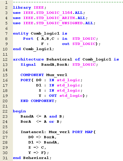
(2) Create a new Schematic Source called "Diagram1"
|
| |
|

|
| |
(3) Draw a circuit like the one
above
(4) Make a synthesize of the Design
(5) Try to implement the Design - A = Sw0, B = Sw1,
C= Sw2, F =Ld0
(6) Download and test the design at the Kit
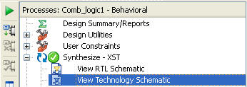
(7) Try the View RTL Schematic
|
| |
 |
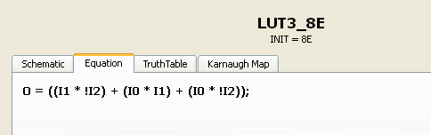
The RTL Schematic Viewer could give a hint of how
the design implemented
(Specially if the design relative simple)
In this case will you get a copy of your own
design (a Look Up Table would have been more
correct)
|
| D |

|
| |
|
| |
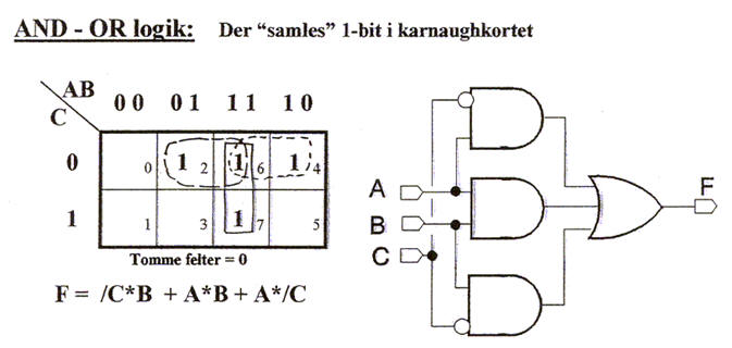
Extra 1 - Try at least one of the
diagrams below and use NAND or NOR logic - just for
the Try.
Extra 2 - Try the same diagram as a VHDL module -
Compare the two solutions with the RTL viewer.
|
| |
|
| |
|
 |
| |
|
|
| |
|
 |
| |
|
|
|
Test Bench and
Simulation
|
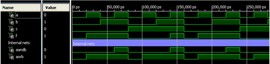
(8) Create a Test Bench - the code
needed shown below
(9) Perform a behavioural simulation
(10) If you want to try Post Place&Route simulation
must you choose the design as Top-level
|
|
 |
| |
|
|
|
| |
|
|
Schematic
Diagram2 - "Multiplexer based solution"
|
(11) Create a solution with the
components shown below
(12) Perform a simulation (Just to make sure)
|
|

Hint |
 |
| |
| |
|
| |
|
|
Schematic
Diagram3 - "Decoder based solution"
|
(13) Create a solution with the
components shown below
(14) Perform a simulation (Just to make sure)
|
|

Hint |

|
| |
| |
|
| |
|
|
Entity with
two Architectures - Merely for demonstration
|
|
|
|
|
|
|
|